









JHY PCB Blog Hub

Your Source for Expert PCB Design, Manufacturing, and Assembly Insights – Stay Informed with 2025 Trends!

10 Best Circuit Board Software for PCB Design?

Choosing Circuit Board Software is not just a matter of picking the tool with the longest feature list. The right program should match your board’s complexity, your team’s workflow, and the way you verify designs. A hobbyist routing a small sensor board needs different tools from an engineer building a dense, high-speed product. Both need dependable results.

PCB design expert Rick Hartley emphasizes a basic principle: “Every signal needs a clear return path.” That idea matters in software selection, too. Strong tools help designers inspect routing, manage layers, check clearances, and catch mistakes before manufacturing. But no feature replaces sound engineering judgment. A polished 3D view can look reassuring while hiding a practical problem. Details matter.

This guide to the 10 Best Circuit Board Software for PCB Design compares popular options by usability, design capabilities, collaboration, and cost. It considers tools for beginners as well as experienced teams, including workflows for schematic capture and board layout. You’ll find the strengths, limitations, and likely use cases of each option. Some differences are subtle. They still matter.

No single package wins for every project. Pricing changes, and a tool that feels intuitive today may frustrate a team later. Treat the shortlist as a starting point, then test your own designs before committing. A small trial board can reveal more than a dozen feature claims.
10 Best Circuit Board Software for PCB Design?

What PCB Design Software Does in Circuit Board Development

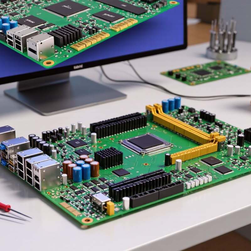
PCB design software connects an electrical idea to a physical circuit board. Engineers draw a schematic, assign component footprints, and define how signals travel between parts. The software then carries those connections into the board layout. A resistor footprint must match its real dimensions, or the finished part may not fit. Small details matter.

During layout, designers place components and route copper traces across one or more board layers. A narrow gap near a connector, for example, can cause a manufacturing problem. Design-rule checks flag issues such as insufficient spacing, unconnected pins, or traces that are too thin. Some tools also simulate circuit behavior, helping engineers examine likely performance before ordering prototypes. These checks help, but they cannot replace careful review.

The software can also create manufacturing files, assembly drawings, and bills of materials. These outputs let fabricators and assembly teams work from consistent design data. Clear naming and notes reduce avoidable questions when a board moves between teams. Still, a green checkmark can create false confidence. Rules depend on the project and manufacturer, and library footprints may contain errors. I would inspect critical footprints against component datasheets, then review the board as if I were assembling it by hand. That extra pass is easy to skip. It can also catch a connector placed too close to an enclosure wall.

How PCB Design Software Supports the PCB Design Process

PCB design software turns an electrical idea into a layout that can be checked, revised, and prepared for fabrication. The process often begins with a schematic, where engineers connect symbols and confirm that power, signals, and component values make sense. Libraries help manage footprints, but they need careful review. A familiar-looking part can still have the wrong pin spacing.

Then the design moves to the board. Engineers arrange components, set layer rules, and route copper paths while watching for clearance and signal-integrity concerns. A 3D view can reveal practical problems, such as a connector facing the wrong edge or a tall part colliding with an enclosure. Small details matter. Design-rule checks flag issues like narrow gaps or unconnected nets, though passing every check does not guarantee a reliable board.

Many tools also support version tracking, team review, and manufacturing-file creation. These features make revisions easier to follow and help keep schematic and layout changes aligned. Simulation can expose likely electrical weaknesses before a prototype is built, but its results depend on accurate models and assumptions. I have seen a tidy layout still need another review; software reduces avoidable errors, not engineering judgment. Before release, teams should inspect the final files and confirm that their layer, drill, and assembly outputs match the fabricator’s requirements.

Key Features to Compare in Circuit Board Design Tools

When comparing circuit board design tools, start with the work your team actually does. Check whether schematic capture and PCB layout share one clear workflow, and whether design-rule checks flag spacing, clearance, and unrouted connections before fabrication. A useful test: place a connector, change its footprint, then inspect how easily the layout updates. Library quality matters. Missing or inconsistent footprints can consume an afternoon.

Look beyond drawing features. Compare simulation options, copper-pour controls, layer management, and output formats accepted by your fabrication partner. Collaboration tools should preserve revision history and make design changes easy to review.

WSTS’s Fall 2024 Semiconductor Market Forecast projected global chip sales of $627.6 billion in 2024, up 19% year over year. That growth underscores why tools need to handle dense, component-rich boards without making routine edits difficult.

Also evaluate learning time, file compatibility, technical support, and the cost of scaling seats or features. Ask whether the software exports manufacturing files reliably, and verify the output with a real design rather than a demo. No tool is perfect. Automated routing can save time, but may still need careful cleanup around sensitive signals. A short trial using one representative board often reveals more than a long feature list.

10 Leading Software Tools for PCB Design

Choosing among ten leading software tools for PCB design is less about glossy dashboards and more about how reliably each handles real board constraints. Grand View Research estimated the global PCB market at USD 73.59 billion in 2023, with projected growth of 5.7% annually from 2024 to 2030. That expansion makes efficient design workflows valuable, but market growth alone does not prove one program is right for every team.

A useful comparison should cover ten distinct needs: beginner-friendly schematic capture, open-source design, cloud collaboration, high-speed routing, RF layout, rigid-flex boards, manufacturing handoff, education, modular ECAD, and enterprise-scale projects. Check whether the software supports design-rule checks, clear component libraries, and dependable fabrication outputs. Then test a small board with a connector, mounting holes, and a tight routing area. Small details matter. A polished 3D view cannot fix a mismatched footprint.

IPC’s design and manufacturing standards also underline why reliable data exchange and manufacturability checks matter. Still, feature lists can mislead; a powerful tool may slow a small team with needless setup. I would compare learning time, collaboration, export quality, and total cost using the same sample design. No single choice wins everywhere. That is easy to say, harder to measure.

10 Best Circuit Board Software for PCB Design? – 10 Leading Software Tools for PCB Design

Software Category Best Suited For Typical Capabilities Common Checks or Outputs Key Consideration
Schematic Capture Creating and documenting circuit connections Places schematic symbols, connects pins, assigns component values, and organizes circuits into sheets. Electrical rule checks and a netlist for PCB layout. Symbol and footprint assignments should be reviewed before board layout.
PCB Layout Editor Placing components and routing a board Defines board outlines, copper layers, component positions, traces, vias, and copper areas. Design rule checks for spacing, connectivity, and board geometry. Routing rules need to match the intended fabrication process.
Integrated Schematic-and-Layout CAD Projects that need coordinated circuit and board changes Links schematic connectivity with physical layout and can support cross-probing between views. Netlist comparison and synchronization checks. Changes in one design view should be synchronized and verified in the other.
High-Density Interconnect (HDI) Design Compact boards with dense component connections Supports fine-pitch routing and, where implemented, microvias, blind or buried vias, and via-in-pad structures. Clearance, via, layer-transition, and manufacturing-rule checks. Fabrication capabilities determine which via structures and feature sizes are practical.
Rigid-Flex Design Boards combining rigid sections with flexible circuits Can define rigid and flex regions, layer stacks, bend areas, and mechanical constraints. Region and stackup checks; some systems provide folded 3D views. Bend limits and material requirements must be confirmed with the fabricator.
High-Speed and RF Design Circuits sensitive to signal integrity or controlled impedance May support differential-pair routing, length constraints, impedance rules, and field-solver integration. Rule-based length and spacing checks; impedance estimates depend on stackup data. Accurate dielectric and copper properties are important for meaningful calculations.
Power Electronics Layout Boards carrying substantial current or managing heat Supports copper sizing, plane areas, thermal reliefs, and placement of power components. Current-density or thermal analysis may be available as an integrated or separate function. Electrical and thermal performance depend on materials, geometry, and operating conditions.
Component Library and Footprint Management Maintaining reusable symbols and land patterns Organizes component symbols, PCB footprints, pin mappings, and associated part data. Library consistency checks and component-to-footprint assignment review. Footprints should be checked against component datasheets and assembly requirements.
Design for Manufacturability (DFM) Checking Finding production-related issues before fabrication Checks design geometry against selected manufacturing constraints, such as spacing and drill rules. Reports potential violations for review and correction. Results are only as relevant as the rules supplied for the intended manufacturing process.
CAM and Manufacturing-Output Tools Preparing board data for fabrication and assembly Views or generates manufacturing files, such as Gerber data and NC drill files; format support varies. Layer, aperture, drill, and output-file review. Confirm the required formats and layer conventions with the board fabricator.

These are software categories rather than vendor-specific products. Features and file-format support vary between implementations.

How to Choose PCB Software for Your Project and Skill Level

Choosing PCB software starts with the board you actually need to build. A simple sensor board may require schematic capture, a few copper layers, and clear design-rule checks. A dense, high-speed design demands tighter control over trace spacing, impedance, and layer stacks. Be realistic about your project’s complexity. More features can mean more menus to learn.

Your skill level matters just as much. Beginners benefit from guided workflows, readable error messages, and libraries that are easy to edit. Experienced designers may prefer flexible routing tools, reusable design blocks, and detailed rule settings. Check whether the software runs smoothly on your computer and supports teamwork if several people will edit the same project. Test the manufacturing-file export, too. A design that looks correct on screen can still contain avoidable errors.

Try a small, representative project before committing. Draw a schematic, place a connector, route a few signals, then run the checks. Notice where you hesitate. That matters. Tutorials and community help can shorten the learning curve, but they cannot fix a confusing workflow for you. I would not choose software based on feature lists alone; honestly, comparing tools takes time, and one trial may not reveal every limitation. Make a short checklist of must-have functions, then compare each option against your budget, experience, and next likely project.

Scroll to Top