


Expert 4 Layer PCB Manufacturer in China - JHYPCB
Discover Professional 4 Layer PCB Stackup, Prototype, and Fabrication Services at Affordable Costs
"At JHYPCB, we specialize in 4-layer PCB manufacturing, delivering high-density, compact solutions for advanced electronics with expert stackup design and affordable prototyping."
JHYPCB Team
Table of Contents
With the growing demand for compact, high-performance electronics, 4-layer PCBs have become essential for achieving smaller, more efficient designs. At JHYPCB, we provide expert 4-layer PCB stackup and prototype services to meet your specific needs, ensuring optimal performance and cost-efficiency.
Want to learn how to design a 4-layer PCB, understand its benefits, or explore its applications? This guide covers everything from stackup design to manufacturing processes, helping you make informed decisions for your next project. Let’s get started!
What Is a 4 Layer PCB? Definition and Basics
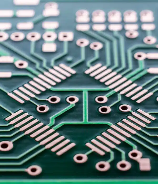
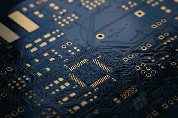
A 4-layer PCB is a type of multilayer printed circuit board featuring four conductive layers, designed to meet the growing demand for high-density and compact electronic devices. Unlike single-layer or double-layer PCBs, a 4-layer PCB includes two inner layers, a top layer, and a bottom layer, offering enhanced functionality for complex circuits.
Curious about PCB classifications? Learn more about the types of PCBs and how they suit your projects.
Specifically, these four layers typically consist of two signal layers for data transmission, one VCC layer for power distribution, and one GND layer for grounding. The inner layers are strategically used as power and ground planes, which minimizes electromagnetic interference (EMI) and improves signal integrity—key advantages for advanced electronics applications.
At JHYPCB, we simplify 4-layer PCB design and manufacturing, offering customized solutions from prototype to full production. Whether you need a standard 4-layer PCB stackup or a tailored design, our expert services ensure optimal performance and reliability.
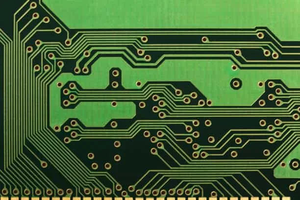
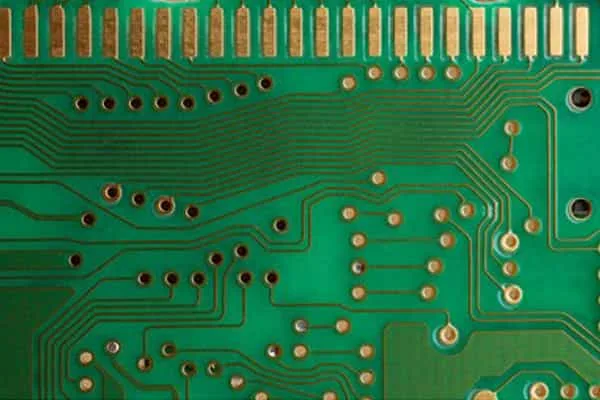
4 Layer PCB Stack up
Standard 4 Layer PCB Stackup Design Guide
A 4-layer PCB stackup is critical for ensuring signal integrity, power distribution, and electromagnetic compatibility in modern electronics. Typically, a 4-layer PCB consists of four conductive layers: a top layer, two inner layers, and a bottom layer. These layers are often configured as two signal layers (top and bottom), one power layer (VCC), and one ground layer (GND). However, the exact stackup can vary depending on your design requirements.
Below are the three most common types of 4-layer PCB stackups:
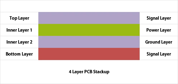
- Standard Stackup (Signal-Power-Ground-Signal): Top layer (signal), Inner Layer 1 (power), Inner Layer 2 (ground), Bottom layer (signal). This configuration balances signal routing and EMI reduction.
- Ground-Signal-Signal-Ground Stackup: Top layer (ground), Inner Layer 1 (signal), Inner Layer 2 (signal), Bottom layer (ground). Ideal for high-speed designs requiring enhanced shielding.
- Signal-Ground-Power-Signal Stackup: Top layer (signal), Inner Layer 1 (ground), Inner Layer 2 (power), Bottom layer (signal). This setup prioritizes grounding proximity to signal layers for better performance.
Choosing the right stackup depends on factors like signal speed, component density, and EMI requirements. At JHYPCB, our engineers can help you design an optimal 4-layer PCB stackup tailored to your project needs, ensuring high performance and manufacturability.

Standard & Typical 4 Layer PCB Stackup
4 Layer PCB Stack up and Layout Guide
Designing an effective 4-layer PCB stackup and layout is crucial for ensuring optimal performance, signal integrity, and manufacturability. This guide builds on the standard 4-layer PCB stackup configurations, providing detailed insights into layer placement, routing, and best practices tailored for your project needs.
At JHYPCB, our expert team leverages advanced manufacturing capabilities to support customized 4-layer PCB layouts. Below, we explore the three key stackup types and their layout considerations:
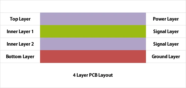
1. First Type of 4 Layer PCB Stackup and Layout
- Stackup: Top Layer – Signal, Inner Layer 1 – Power, Inner Layer 2 – Ground, Bottom Layer – Signal
- Layout Tips: Place signal traces on the outer layers for easy access. Ensure the power and ground planes are closely spaced to minimize impedance and enhance EMI shielding.
- Best For: General-purpose designs requiring balanced signal routing and power distribution.
The close proximity of power and ground layers improves decoupling, but a thicker core or prepreg may require careful impedance matching.
The first type of 4 layer PCB stack up
2. Second Type of 4 Layer PCB Stackup and Layout
- Stackup: Top Layer – Power, Inner Layer 1 – Signal, Inner Layer 2 – Signal, Bottom Layer – Ground
- Layout Tips: Route high-speed signals on inner layers to reduce EMI. Use the top power layer for decoupling capacitors and the bottom ground layer as a reference plane.
- Best For: High-speed applications where shielding and signal integrity are critical.
This setup offers robust EMI protection due to the shielding effect of power and ground planes, though component placement near the edges requires attention.
The second type of 4 layer PCB stack up
3. Third Type of 4 Layer PCB Stackup and Layout
- Stackup: Top Layer – Signal, Inner Layer 1 – Ground, Inner Layer 2 – Power, Bottom Layer – Signal
- Layout Tips: Prioritize ground plane proximity to signal layers for better noise reduction. Route power planes to avoid interference with high-density components.
- Best For: Complex designs with high component density and stringent grounding needs.
This configuration enhances signal quality but may limit top-layer accessibility, requiring optimized via placement.
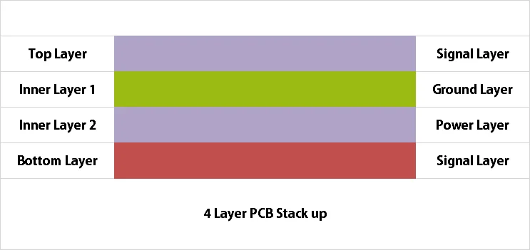
The third type of 4 layer PCB stack up
Choosing the right stackup and layout depends on your project’s specifications, such as signal speed and EMI tolerance. JHYPCB offers tailored 4-layer PCB design and prototyping services to ensure your layout meets industry standards.
For more layout tips and stackup examples, download our comprehensive guide: Click here for the 4-16 Layer PCB Stackup and Layout Guide.
Need help with 4-layer PCB design? Download our free tutorials for popular PCB design software to get started:
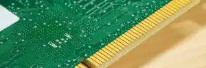
4 Layer PCB Core and Prepreg Thickness
The core and prepreg thickness in a 4-layer PCB stackup play a critical role in determining signal integrity, impedance control, and overall board reliability. The core is the central layer of solid laminate, while prepreg (pre-impregnated fiberglass) bonds the layers together, affecting the final 4-layer PCB thickness and performance.
At JHYPCB, we optimize core and prepreg thickness to meet your design specifications, ensuring high-quality 4-layer PCB manufacturing. Here’s a breakdown of their impact:
- Core Thickness: Typically ranges from 0.2mm to 1.6mm, depending on the board’s rigidity and layer count. Thicker cores enhance structural stability but may increase weight and cost.
- Prepreg Thickness: Usually varies from 0.1mm to 0.4mm per layer. Thinner prepreg improves signal coupling between power and ground planes, reducing EMI, while thicker prepreg provides better insulation.
The combined thickness of core and prepreg influences impedance matching and decoupling efficiency. For example, a standard 4-layer PCB stackup might use a 0.8mm core with 0.2mm prepreg on each side, totaling approximately 1.2mm. JHYPCB’s advanced equipment ensures precise control over these parameters for optimal performance.
Related Reading:
Why Use a 4 Layer PCB? Key Advantages
Compared to single-layer or double-layer PCBs, a 4-layer PCB offers significant advantages, making it a preferred choice for modern electronics requiring high performance and compact designs. While 4-layer PCBs may have a higher initial cost, their benefits in signal integrity, EMI shielding, and thermal management often justify the investment. Here’s why you should consider a 4-layer PCB for your next project:
- Enhanced Signal Integrity: A 4-layer PCB stackup allows for dedicated signal layers, reducing noise and crosstalk. Inner layers can be used for power and ground planes, ensuring stable signal transmission, especially for high-speed circuits.
- Superior EMI Shielding: The ground and power planes in a 4-layer PCB act as a shield, minimizing electromagnetic interference (EMI). This is crucial for applications like telecommunications and medical devices, where reliability is paramount.
- Improved Thermal Management: The layered design of a 4-layer PCB distributes heat evenly across the board, preventing hotspots. This enhances the longevity of components, especially in high-power applications.
- Increased Assembly Density: With four layers, a 4-layer PCB supports higher component density, allowing more complex circuits in a smaller footprint. This is ideal for compact devices like wearables and IoT gadgets.
- Compact and Lightweight Design: By stacking layers vertically, 4-layer PCBs reduce the overall board size, enabling sleeker, more portable electronic products without compromising functionality.
At JHYPCB, we specialize in manufacturing high-quality 4-layer PCBs tailored to your specifications, ensuring all these advantages are maximized for your project. Curious about how a 4-layer PCB compares to a 2-layer PCB? Explore our comparison guide.
Ready to leverage the benefits of a 4-layer PCB? Request a quote from JHYPCB today and start your project with confidence!
4 Layer PCB Applications in Modern Electronics
4-layer PCBs are widely used across various industries due to their ability to support complex circuits, enhanced signal integrity, and compact designs. Their multilayer structure makes them ideal for applications requiring high performance and reliability. Here’s a look at where 4-layer PCBs excel:
- Telecommunications: 4-layer PCBs are essential in devices like routers, base stations, and satellite systems, where they ensure stable signal transmission and EMI shielding for high-speed data transfer.
- Consumer Electronics: From smartphones to wearable devices, 4-layer PCBs enable compact designs with higher component density, supporting advanced features in smaller footprints.
- Medical Devices: In equipment like MRI machines and patient monitoring systems, 4-layer PCBs provide reliable performance, minimizing noise and ensuring precision in critical applications.
- Automotive Systems: Used in engine control units (ECUs) and infotainment systems, 4-layer PCBs handle high-power requirements and thermal stress, ensuring durability in harsh environments.
- Industrial Automation: In robotics and control systems, 4-layer PCBs support complex circuitry, offering improved thermal management and signal integrity for seamless operation.
At JHYPCB, we’ve empowered countless industries with high-quality 4-layer PCB manufacturing, from prototypes to full production. Our advanced capabilities ensure your application-specific needs are met with precision and efficiency.
Want to explore how a 4-layer PCB can enhance your project? Contact JHYPCB for a free application consultation today!
2 Layer vs. 4 Layer PCB: A Comparison
Choosing between a 2-layer PCB and a 4-layer PCB depends on your project’s complexity, performance requirements, and budget. While 2-layer PCBs are cost-effective for simpler designs, 4-layer PCBs offer superior functionality for advanced applications. Here’s a detailed comparison to help you decide:
| Feature | 2-Layer PCB | 4-Layer PCB |
|---|---|---|
| Layer Count | 2 layers (top and bottom) | 4 layers (top, bottom, and two inner layers) |
| Signal Integrity | Limited; prone to noise and crosstalk | Enhanced; dedicated power and ground planes reduce noise |
| EMI Shielding | Minimal; lacks dedicated shielding layers | Superior; ground planes minimize electromagnetic interference |
| Component Density | Lower; limited space for complex circuits | Higher; supports more components in a compact footprint |
| Thermal Management | Poor; heat dissipation is limited | Better; layered design distributes heat evenly |
| Cost | Lower; ideal for budget-sensitive projects | Higher; but offers better performance for the investment |
| Applications | Simple devices (e.g., basic sensors, calculators) | Advanced systems (e.g., smartphones, medical devices) |
While 2-layer PCBs are suitable for basic applications, 4-layer PCBs excel in scenarios requiring high performance, such as telecommunications, automotive, and IoT devices. At JHYPCB, we specialize in 4-layer PCB manufacturing, offering customized solutions to meet your specific needs, from design to production.
Not sure which PCB type is right for your project? Contact JHYPCB for a free consultation and get expert advice tailored to your application!
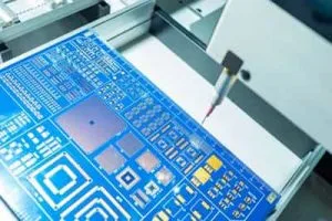
4 Layer PCB Prototype Service by JHYPCB
JHYPCB offers top-tier 4-layer PCB prototype services, delivering fast, reliable, and cost-effective solutions for your design validation needs. Whether you’re developing a new product or testing a complex circuit, our prototyping expertise ensures your 4-layer PCB meets the highest standards before full production.
- Fast Turnaround: Receive your 4-layer PCB prototype in as little as 24-48 hours with our expedited service.
- Customizable Options: Tailor stackup, thickness, and materials to match your project requirements.
- Quality Assurance: Rigorous testing ensures optimal signal integrity, EMI shielding, and thermal performance.
- Cost-Effective: Competitive pricing for prototypes, ideal for startups and small-batch projects.
Our prototype process includes design review, material selection, stackup configuration, and final testing—all handled by our experienced team in China. This ensures a seamless transition from prototype to mass production.
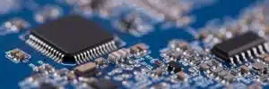
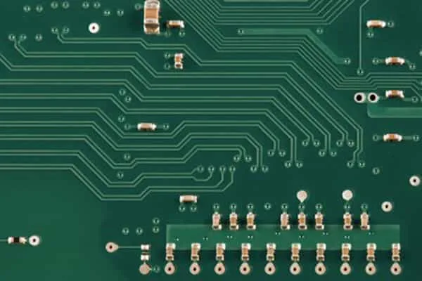
4 Layer PCB Manufacturing
How to Make a 4 Layer PCB: Step-by-Step Process
Creating a 4-layer PCB involves a precise manufacturing process to ensure high-quality results, from design to final assembly. Whether you’re a hobbyist or an engineer, understanding the steps can help you optimize your 4-layer PCB design. At JHYPCB, we streamline this process with advanced technology and expertise in China.
- Design and Layout: Use PCB design software (e.g., Altium Designer or KiCad) to create a schematic and layout, defining the stackup with signal, power, and ground layers.
- Material Selection: Choose core and prepreg materials based on thickness and dielectric properties to meet impedance and thermal requirements.
- Layer Lamination: Stack and bond the four layers (top, inner power, inner ground, bottom) using heat and pressure, with prepreg as the adhesive layer.
- Drilling and Plating: Drill holes for vias and through-holes, then plate them with copper to connect layers electrically.
- Etching and Imaging: Apply a photoresist, expose it to UV light, and etch away excess copper to form the circuit patterns.
- Testing and Quality Check: Conduct electrical tests and inspections to ensure signal integrity, EMI shielding, and compliance with specifications.
- Final Assembly: Add surface finishes (e.g., HASL or ENIG) and components, preparing the PCB for use or mass production.
JHYPCB’s state-of-the-art manufacturing facility ensures each step is executed with precision, offering fast turnarounds and reliable 4-layer PCB production. Our process supports both prototypes and large-scale orders, tailored to your needs.
Want to manufacture your own 4-layer PCB? Get started with JHYPCB’s expert manufacturing services today!
4 Layer PCB Cost Factors Explained
The cost of a 4-layer PCB depends on several key factors, making it higher than a 2-layer PCB but justifiable for its enhanced performance. Understanding these factors can help you optimize your budget while achieving the best results. At JHYPCB, we offer competitive pricing for 4-layer PCB manufacturing and prototyping in China.
- Layer Count and Complexity: A 4-layer PCB requires more materials and manufacturing steps than a 2-layer PCB, increasing costs based on design complexity.
- Material Selection: The choice of core thickness (e.g., 0.8mm) and prepreg (e.g., 0.2mm) impacts cost, with high-quality materials adding to the expense.
- Board Size and Quantity: Larger boards or smaller production runs (e.g., prototypes) tend to be more expensive per unit, while bulk orders reduce the cost per PCB.
- Manufacturing Process: Advanced techniques like multi-layer lamination, drilling, and plating contribute to costs, especially for high-precision designs.
- Surface Finish: Options like HASL or ENIG affect pricing, with gold finishes (ENIG) being more costly than lead-free HASL.
For example, a standard 4-layer PCB prototype (100mm x 100mm, 1.2mm thickness) might range from $50 to $150 depending on these factors, with JHYPCB offering cost-effective solutions tailored to your needs. Our streamlined process and advanced equipment help minimize costs without compromising quality.
Need an accurate cost estimate for your 4-layer PCB? Request a free quote from JHYPCB today and optimize your project budget!
Get Your 4 Layer PCB from JHYPCB in China
As a leading 4-layer PCB manufacturer in China, JHYPCB delivers high-quality, reliable, and cost-effective PCB solutions for projects of all sizes. From rapid prototyping to large-scale production, our advanced manufacturing capabilities and strict quality control ensure your 4-layer PCB meets industry standards and your specific requirements.
- Why Choose JHYPCB?
- Fast delivery: Prototypes in as little as 24-48 hours.
- Competitive pricing: Affordable rates for both small and bulk orders.
- Expert support: Free design reviews and consultations.
- Global reach: Trusted by clients worldwide, with seamless shipping.
With over a decade of experience, JHYPCB is your trusted partner for 4-layer PCB fabrication, whether you need a single prototype or a wholesale order. Let us bring your design to life with precision and efficiency.
4 Layer PCB FAQs
Got questions about 4-layer PCBs? We’ve compiled answers to the most common queries to help you understand their design, manufacturing, and benefits. At JHYPCB, we’re here to support your 4-layer PCB journey from start to finish.
What is the typical thickness of a 4-layer PCB?
A standard 4-layer PCB thickness ranges from 0.8mm to 1.6mm, depending on the core and prepreg materials used. For example, a common stackup might include a 0.8mm core with 0.2mm prepreg per layer, totaling around 1.2mm. JHYPCB can customize the thickness to meet your specific design requirements.
How does a 4-layer PCB improve signal integrity?
A 4-layer PCB improves signal integrity by using dedicated power and ground planes, which reduce noise and crosstalk. The inner layers stabilize signal transmission, making it ideal for high-speed applications like telecommunications and medical devices.
What are the main applications of 4-layer PCBs?
4-layer PCBs are widely used in industries such as consumer electronics (e.g., smartphones), automotive (e.g., ECUs), medical devices (e.g., MRI machines), and industrial automation (e.g., robotics), thanks to their compact design and enhanced performance.
How much does a 4-layer PCB prototype cost?
The cost of a 4-layer PCB prototype varies based on size, materials, and complexity, typically ranging from $50 to $150 for a 100mm x 100mm board. JHYPCB offers competitive pricing and free quotes to help you manage your budget.
How long does it take to manufacture a 4-layer PCB prototype?
At JHYPCB, we provide fast turnarounds, with 4-layer PCB prototypes available in as little as 24-48 hours for expedited orders. Standard lead times typically range from 5 to 7 days, depending on order volume and specifications.
Still have questions? Contact JHYPCB for personalized support and get expert guidance for your 4-layer PCB project!
Related PCB Board Fabrication Service
Rigid PCB is a Traditional printed circuit board, one of the most used and produced PCBs.
It can realize 3D three-dimensional assembly, which is completely different from rigid PCB.
The excellent combination of rigid PCB and flexible PCB realizes an incredible experience.
Single-sided or single-layer PCB is the simplest circuit board, but they are still widely used.
The 6-layer PCB has more wiring layers, allowing a higher-precision device design.
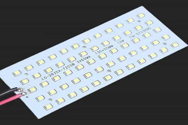
LED PCB boards are widely used in the lighting industry, such as plant growth lights.
Related Posts
- What is a Multilayer PCB and What are the Advantages?
- Angle Control in Multilayer PCB
- Custom Circuit Board Printing
- Top PCB Board Manufacturer And Supplier In China
- The Best And Fastest PCB Manufacturer In China
- Custom PCB Manufacturer In China
- Why Choose Chinese PCB Manufacturer
- How to Store PCB and PCBA?
- What Is FR-4 Material In PCB Fabrication?
- What Are the Multilayer PCB Applications?