
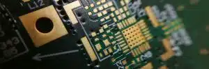


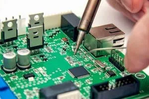
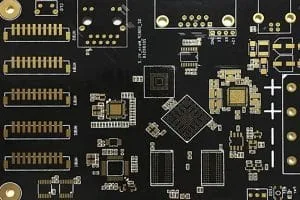
What is a Pad in PCB Design?
What are pads in PCBs and why are they so important for electronics design and manufacturing? This definitive guide covers
Understanding Plated Half-Holes (Castellated Holes) in PCB Design
Plated half-holes, also called castellated holes, provide a space-efficient way to interconnect separate PCB modules by soldering. Unlike bottom pads,
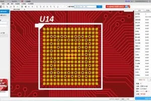
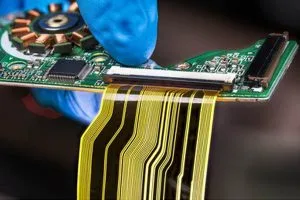
Identifying and Processing Via-In-Pad in PCB Design
Via-in-pad refers to drilling vias on pads, commonly used for high density SMD and BGA pads. This article covers in
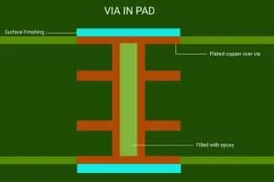
An Introduction to Via-in-Pad for Printed Circuit Boards
Via-in-pad technology for PCBs places vias directly within surface mount pads, conserving space by merging interconnect structures. Learn benefits and
Leveraging Filled and Capped Vias for Enhanced PCB Reliability
Filled and capped vias are advanced PCB design techniques that measurably enhance connection reliability. Learn when and why to leverage
What are Tented Vias? A Guide to This Important PCB Feature
What are tented vias and why should PCB designers use them? Read our full guide covering how tented vias work,

Blind Vias, Buried Vias in PCBs – A Complete Guide
Blind vias and buried vias enable improved signal routing, component density, performance, and simplified PCB stackups essential for complex, high-speed

Understanding Plated Through Holes (PTH) for Printed Circuit Boards
Plated through holes (PTHs) are vital in printed circuit boards for enabling reliable connectivity between layers. This article explores PTHs
An Overview of Vias in Printed Circuit Boards
Vias enable complex functionality in printed circuit boards by facilitating vertical transitions between layers. This article provides an overview of
The Essentials of Microvias – Enabling Miniaturization in PCBs
As printed circuit boards are designed to pack more components into increasingly compact spaces, microvias play a crucial role in
Layer Stackup in Rigid-Flex PCB
A rigid-flex PCB Stackup is a type of PCB that has both rigid and flexible layers. You should choose the
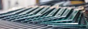
Guide to Multilayer PCB Layer Stackup and thickness
PCB Stack-up refers to the arrangement of copper layers and insulating layers that make up a PCB prior to board
PCB Stackup Design Guidelines and Considerations
As a professional PCB manufacturer, we have summarized the following PCB stacking design guidelines and precautions in practical applications, hoping
A Free Software for PCB Design for Manufacturing or DFM Analysis
PCB design is a complete and rigorous process system, and PCB manufacturing is another set of sophisticated production and processing
4 Solutions to Reduce EMC in 6-layer PCB Design
In the EMC design of the PCB, the first important thing is the setting of the layers. The number of
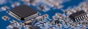
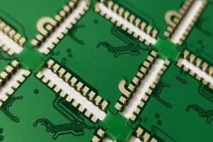
Basic Knowledge of PCB Pad Design
When laying out PCB components, designers should consider the difference between the minimum spacing between components relative to the thickness
HDI PCB Layout and Basic HDI Design Guidelines
HDI circuit board is an advanced printed circuit board. If you suspect you’ll need to work with component densities that
PCB Design Guidelines
Printed circuit boards have become a fundamental factor in developing contemporary electronic products. Printed circuit boards are one of the
Angle Control in Multilayer PCB
Multilayer PCB fabrication is a sophisticated process, mainly when many layers are involved on a small sizing motherboard.
10 Tips To Improve PCB Design For Manufacturability
Through the Design For Manufacturability(DFM) of the printed circuit board, the design department and the production department can be effectively
What are the aspects of PCB Design For Manufacturing (DFM) and Design For Assembly (DFA)?
This article will introduce in detail about what is PCB Design For Manufacturing (DFM) And Design For Assembly (DFA).
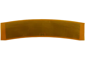
5 Key Factors for FPC PCB Impedance Control Success
Impedance control is critical for high-performance FPC PCBs in 5G, IoT, and automotive applications. Learn five key factors—substrate properties, trace