


Table of Contents
Introduction
In the fast-evolving world of electronics, Flexible Printed Circuit Boards (FPCs) are at the heart of cutting-edge applications like 5G telecommunications, Internet of Things (IoT) devices, and automotive electronics. These flexible circuits offer unparalleled design versatility, but their performance hinges on one critical factor: impedance control. Why is impedance control so vital for FPC PCBs? Without precise management of impedance, high-speed signals can degrade, leading to data errors, reduced performance, or even system failure in mission-critical applications.
Impedance control ensures that signals travel efficiently through the circuit with minimal distortion, making it essential for high-frequency designs. However, achieving consistent impedance in FPCs is no small feat. The flexible nature of these circuits, combined with material and manufacturing complexities, introduces unique challenges for PCB designers. In this article, we explore five key factors that every FPC PCB designer must understand to master impedance control and deliver reliable, high-performance circuits.
Whether you’re designing compact wearables or advanced automotive systems, understanding these factors—ranging from substrate material properties to manufacturing tolerances—will empower you to optimize signal integrity and meet stringent performance requirements. Let’s dive into the essentials of FPC PCB impedance control and discover how partnering with an experienced manufacturer like JHYPCB can make all the difference.
Understanding Impedance Control in FPC PCBs
What is Impedance Control?
Impedance control in Flexible Printed Circuit Boards (FPCs) refers to the precise management of the electrical impedance of circuit traces to ensure reliable signal transmission, especially in high-speed and high-frequency applications. Impedance, measured in ohms (Ω), represents the opposition to alternating current (AC) flow in a circuit. In FPC designs, maintaining a consistent characteristic impedance (( Z_0 )) is critical to preventing signal reflections, crosstalk, and data loss, which can compromise the performance of devices like smartphones, wearables, and automotive control systems.
The characteristic impedance of a trace is determined by its physical properties and the surrounding materials, as described by the formula:
[ Z_0 = \sqrt{\frac{L}{C}} ]
where ( L ) is the inductance per unit length (in henries per meter) and ( C ) is the capacitance per unit length (in farads per meter). By carefully designing the trace geometry and selecting appropriate materials, designers can achieve the desired impedance, typically 50Ω for single-ended signals or 100Ω for differential pairs in FPC applications.
Why is Impedance Control Critical for FPC PCBs?
Unlike rigid PCBs, FPCs are highly flexible, lightweight, and often used in compact, high-density designs. These characteristics make impedance control both essential and challenging. Here’s why:
- High-Speed Signal Integrity: In applications like 5G antennas or USB 3.0 interfaces, even minor impedance mismatches can cause signal reflections, leading to data errors or reduced transmission speeds.
- Flexibility and Bending: FPCs are subject to bending and folding, which can alter trace geometry and affect impedance. Proper design ensures stability under dynamic conditions.
- Miniaturization: FPCs are often used in space-constrained devices, requiring precise trace layouts to maintain impedance in tight spaces.
- High-Frequency Performance: As frequencies increase (e.g., in RF or high-speed digital circuits), impedance control becomes more critical to minimize signal distortion.
Challenges in FPC Impedance Control
Achieving consistent impedance in FPCs is more complex than in rigid PCBs due to several factors:
Material Variability: Flexible substrates like polyimide have varying dielectric constants, which can affect impedance if not carefully selected.
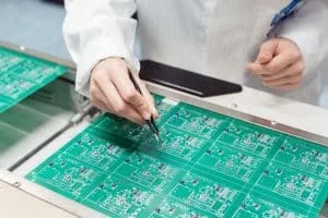
Manufacturing Tolerances: Processes like etching and copper plating must be tightly controlled to maintain precise trace dimensions.
Dynamic Environments: FPCs may bend or flex during operation, requiring robust designs to ensure impedance stability.
To address these challenges, designers must consider substrate properties, trace geometry, and manufacturing processes—topics we’ll explore in the next section. By mastering these factors, you can ensure optimal signal integrity in your FPC designs, and partnering with an experienced manufacturer like JHYPCB can help you navigate these complexities with precision.
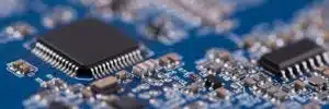
Five Key Factors Affecting Impedance Control in FPC PCBs
Achieving precise impedance control in Flexible Printed Circuit Boards (FPCs) requires careful consideration of multiple design and manufacturing factors. The following five elements play a critical role in determining the impedance of FPC traces and ensuring signal integrity in high-speed applications. By understanding and optimizing these factors, designers can create reliable, high-performance FPC PCBs.
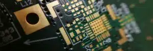
3.1 Substrate Material Properties
The substrate material is the foundation of an FPC and significantly influences its impedance. The dielectric constant (Dk) and dissipation factor (Df) of the substrate determine how electrical signals propagate through the circuit. Common FPC substrates, such as polyimide (Dk ≈ 3.2–3.5) and polyethylene terephthalate (PET, Dk ≈ 3.0), have distinct dielectric properties that directly affect the characteristic impedance (( Z_0 )).
Why It Matters: Variations in Dk across a substrate can lead to impedance mismatches, causing signal reflections and data errors. Consistent material properties are essential for predictable performance.
Design Tip: Select substrates with stable Dk values and low Df to minimize signal loss, especially in high-frequency applications like 5G or RF circuits.
JHYPCB Expertise: At JHYPCB, we offer a range of high-quality polyimide substrates with well-characterized dielectric properties to ensure reliable impedance control.
Table: Common FPC Substrate Materials and Their Dielectric Properties
Material | Dielectric Constant (Dk) | Typical Applications |
|---|---|---|
Polyimide | 3.2–3.5 | High-speed, flexible electronics |
PET | 2.8–3.0 | Cost-sensitive, low-frequency designs |
Liquid Crystal Polymer (LCP) | 2.9–3.1 | Ultra-high-frequency RF circuits |
Internal Link: Explore JHYPCB’s material selection guide for FPC PCBs.
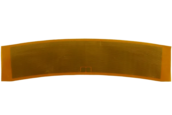
3.2 Trace Thickness and Width
The physical dimensions of the conductive traces—specifically their width and thickness—directly impact the impedance of an FPC. The characteristic impedance is inversely proportional to trace width, as shown in the simplified relationship for microstrip lines:
[ Z_0 \propto \frac{1}{W} ]
where ( W ) is the trace width. Similarly, trace thickness affects resistance and, indirectly, impedance.
Why It Matters: Wider traces reduce impedance but may compromise flexibility, while thinner traces increase impedance and resistance, potentially affecting signal strength.
Design Tip: Use PCB design software to calculate optimal trace width and thickness based on target impedance (e.g., 50Ω for single-ended signals). Balance flexibility and performance for dynamic FPC applications.
JHYPCB Expertise: Our advanced manufacturing processes ensure precise trace dimensions to meet your impedance requirements.
Figure: Diagram showing the relationship between trace width and impedance in an FPC microstrip configuration.
3.3 Trace Spacing and Electromagnetic Interference
Trace spacing in FPC designs affects not only impedance but also electromagnetic interference (EMI) and crosstalk between adjacent traces. Closely spaced traces generate magnetic fields that can induce unwanted currents, altering the effective impedance and degrading signal integrity.
Why It Matters: In high-density FPC layouts, insufficient spacing can lead to crosstalk, especially in high-speed differential pair designs (e.g., 100Ω differential impedance).
Design Tip: Optimize trace spacing based on IPC-2223 standards for flexible circuits. Incorporate ground planes or shielding layers to minimize EMI in sensitive applications.
JHYPCB Expertise: We provide advanced shielding solutions and precise trace layouts to reduce EMI and ensure consistent impedance.
Internal Link: Learn about JHYPCB’s EMI shielding solutions for FPC PCBs.
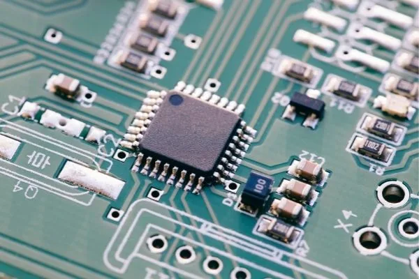
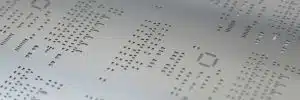
3.4 Etching Tolerance and Process Control
The etching process, which defines the trace geometry, is critical for achieving accurate impedance in FPCs. Etching removes excess copper to form traces, but variations in etching tolerance (typically ±10–20% for standard processes) can alter trace width and thickness, impacting impedance.
Why It Matters: Inconsistent etching can lead to impedance deviations, especially in high-precision applications requiring tight tolerances (e.g., ±5Ω).
Design Tip: Collaborate with your manufacturer to specify etching tolerances and validate designs using Time Domain Reflectometry (TDR) during prototyping.
JHYPCB Expertise: JHYPCB employs advanced etching techniques to achieve tight tolerances, ensuring precise impedance control for your FPC designs.
Case Study: Read how JHYPCB achieved ±3% etching tolerance for a high-speed FPC project.
3.5 Copper Plating Consistency
Copper plating, used to enhance trace conductivity and durability, can introduce impedance variations if not applied uniformly. In FPCs, copper is typically plated after etching, which can slightly alter trace dimensions and affect impedance.
Why It Matters: Non-uniform plating thickness can change the effective resistance and impedance of traces, particularly in high-frequency circuits where skin effect becomes significant.
Design Tip: Specify controlled electroplating processes and verify plating uniformity during manufacturing to maintain consistent impedance.
JHYPCB Expertise: Our state-of-the-art plating facilities ensure uniform copper deposition, delivering reliable impedance control for FPC PCBs.
Internal Link: Discover JHYPCB’s advanced plating capabilities for flexible circuits.
Practical Tips for Optimizing Impedance Control in FPC Design
Mastering impedance control in Flexible Printed Circuit Boards (FPCs) requires a combination of careful design, precise manufacturing, and thorough validation. Whether you’re designing FPCs for high-speed telecommunications, wearable devices, or automotive systems, the following practical tips will help you achieve reliable impedance control and ensure optimal signal integrity. By implementing these strategies and partnering with an experienced manufacturer like JHYPCB, you can streamline your design process and deliver high-performance FPC PCBs.
1. Use PCB Design Software for Impedance Simulation
Modern PCB design tools, such as Altium Designer, Cadence Allegro, or Ansys SIwave, allow you to simulate impedance during the design phase, reducing the risk of costly revisions. These tools calculate characteristic impedance (( Z_0 )) based on trace geometry, substrate properties, and stack-up configuration.
How to Implement: Input your substrate’s dielectric constant (Dk), trace width, thickness, and spacing into the software to model impedance for microstrip or stripline configurations. For example, a 50Ω single-ended trace on a polyimide substrate (Dk ≈ 3.4) typically requires a trace width of 0.1–0.2 mm, depending on the stack-up.
Pro Tip: Simulate impedance under dynamic conditions (e.g., bending or flexing) to ensure stability in flexible applications.
JHYPCB Support: Our design consultation team can assist with impedance modeling and recommend optimal stack-ups for your FPC project.
Internal Link: Learn how JHYPCB’s design services optimize FPC performance.
2. Collaborate Early with Your Manufacturer
Engaging with your FPC manufacturer early in the design process ensures alignment on material selection, manufacturing tolerances, and impedance requirements. Manufacturers like JHYPCB can provide insights into substrate availability, etching precision, and plating processes that impact impedance.
How to Implement: Share your impedance specifications (e.g., 50Ω single-ended or 100Ω differential) and application requirements with your manufacturer during the design phase. Request material data sheets and process capabilities to inform your design choices.
Pro Tip: Ask for a manufacturability review to identify potential impedance control issues before prototyping.
JHYPCB Support: JHYPCB offers Design for Manufacturability (DFM) reviews to ensure your FPC designs meet impedance and performance goals.
Internal Link: Request a DFM review from JHYPCB.
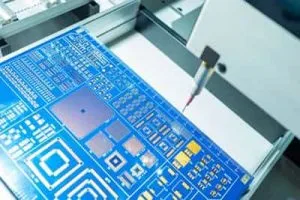
3. Perform Time Domain Reflectometry (TDR) Testing
Time Domain Reflectometry (TDR) is a powerful method for validating impedance during prototyping. TDR measures the reflections of a fast electrical pulse along a trace, providing a direct assessment of impedance consistency across the FPC.
How to Implement: Use a TDR instrument to measure impedance variations along traces, ensuring they meet your target (e.g., ±5Ω for high-precision designs). Test prototypes under static and dynamic (flexed) conditions to verify performance.
Pro Tip: Combine TDR with simulation results to identify discrepancies and refine your design or manufacturing process.
JHYPCB Support: Our prototyping services include TDR testing capabilities to validate impedance control before full-scale production.
Internal Link: Explore JHYPCB’s prototyping services for FPC PCBs.
4. Optimize Stack-Up Design for Impedance Control
The stack-up configuration of an FPC—whether microstrip (single ground plane) or stripline (dual ground planes)—significantly affects impedance. Proper stack-up design ensures consistent impedance while accommodating the flexibility requirements of FPCs.
How to Implement: Use a stack-up calculator to determine layer thickness, dielectric properties, and trace placement. For example, a stripline configuration typically offers better EMI shielding but may increase thickness, while a microstrip is simpler but more susceptible to external interference.
Pro Tip: Incorporate ground planes or shielding layers to stabilize impedance and reduce electromagnetic interference (EMI) in high-speed designs.
JHYPCB Support: JHYPCB’s engineering team can recommend customized stack-ups tailored to your impedance and flexibility needs.
Figure: Diagram of microstrip vs. stripline configurations in FPC designs.
5. Document and Validate Impedance Specifications
Clearly document your impedance requirements in your design files and communicate them to your manufacturer. Validation during manufacturing ensures that the final FPC meets your specifications.
How to Implement: Specify impedance targets (e.g., 50Ω ± 10%) and tolerances in your Gerber files and fabrication notes. Request impedance test reports from your manufacturer to confirm compliance.
Pro Tip: Use controlled impedance test coupons during manufacturing to monitor process consistency without sacrificing production boards.
JHYPCB Support: JHYPCB provides detailed impedance test reports and uses advanced quality control processes to ensure your FPCs meet exact specifications.
Downloadable Resource: Get JHYPCB’s Impedance Control Checklist for FPC Design.
Why Choose JHYPCB for FPC Impedance Control?
Designing and manufacturing Flexible Printed Circuit Boards (FPCs) with precise impedance control demands expertise, advanced technology, and a commitment to quality. At JHYPCB, we specialize in delivering high-performance FPC PCBs tailored to your exact specifications, ensuring optimal signal integrity for applications like 5G telecommunications, IoT devices, and automotive electronics. Here’s why JHYPCB is your trusted partner for achieving reliable impedance control in FPC designs.
1. Proven Expertise in FPC Manufacturing
With years of experience in producing flexible, rigid, and rigid-flex PCBs, JHYPCB understands the complexities of impedance control. Our team of engineers and technicians is well-versed in designing and manufacturing FPCs that meet stringent impedance requirements, such as 50Ω single-ended or 100Ω differential pairs, for high-speed and high-frequency applications.
What We Offer: Comprehensive support from design consultation to final production, ensuring your FPC meets impedance and performance goals.
Example: We’ve successfully delivered FPCs for RF modules in 5G antennas, maintaining tight impedance tolerances (±5Ω) for superior signal integrity.
Internal Link: Discover JHYPCB’s expertise in flexible PCB manufacturing.
2. Advanced Manufacturing Capabilities
JHYPCB’s state-of-the-art facilities are equipped with cutting-edge technology to ensure precise impedance control. From high-precision etching to uniform copper plating, our manufacturing processes are optimized to minimize variations and deliver consistent results.
Key Capabilities:
Precision Etching: Achieve etching tolerances as tight as ±3% to maintain accurate trace geometry.
Controlled Plating: Ensure uniform copper deposition for reliable impedance and durability.
Material Expertise: Access to high-quality substrates like polyimide and LCP with stable dielectric properties (Dk ≈ 3.2–3.5).
Benefit: Our advanced processes reduce impedance deviations, ensuring your FPCs perform reliably in demanding applications.
Internal Link: Learn about JHYPCB’s advanced manufacturing capabilities.
3. Comprehensive Quality Assurance
Quality is at the core of JHYPCB’s operations. We implement rigorous quality control measures to validate impedance and ensure your FPCs meet industry standards, such as IPC-2223 for flexible circuits.
What We Offer:
Time Domain Reflectometry (TDR) testing to verify impedance during prototyping and production.
Detailed test reports documenting impedance compliance (e.g., ±10% for standard designs, ±5% for high-precision projects).
Use of test coupons to monitor manufacturing consistency without sacrificing production boards.
Benefit: Our quality assurance processes give you confidence that your FPCs will perform as expected in real-world conditions.
Case Study: See how JHYPCB ensured impedance accuracy for a high-speed IoT device.
4. Customized Solutions and Fast Turnaround
Every FPC project is unique, and JHYPCB offers customized solutions to meet your specific impedance and design requirements. Whether you need a single-layer FPC for a compact wearable or a multilayer design for automotive applications, we tailor our processes to your needs.
What We Offer:
Design for Manufacturability (DFM) reviews to optimize impedance control early in the design phase.
Rapid prototyping services to accelerate your development timeline.
Flexible production scales, from low-volume prototypes to high-volume manufacturing.
Benefit: Our customized approach and fast turnaround times help you bring your FPC designs to market quickly and efficiently.
Internal Link: Request a custom FPC PCB quote from JHYPCB.
5. Dedicated Customer Support
At JHYPCB, we believe in building strong partnerships with our clients. Our dedicated customer support team is available to guide you through every step of the FPC design and manufacturing process, from material selection to final delivery.
What We Offer: Expert consultation on impedance control, stack-up design, and material choices to ensure your project’s success.
Benefit: Our responsive support team helps you overcome challenges and achieve your design goals with confidence.
Conclusion
Impedance control is a cornerstone of high-performance Flexible Printed Circuit Board (FPC) design, ensuring reliable signal integrity in applications ranging from 5G telecommunications to IoT devices to automotive systems. In this article, we’ve explored five key factors that FPC PCB designers must master to achieve precise impedance control: substrate material properties, trace thickness and width, trace spacing and EMI, etching tolerance, and copper plating consistency. By carefully addressing these factors, designers can create FPCs that deliver optimal performance in high-speed and high-frequency environments.
Partnering with an experienced manufacturer like JHYPCB is essential to overcoming the challenges of FPC impedance control. With advanced manufacturing capabilities, rigorous quality assurance, and expert support, JHYPCB ensures your FPCs meet stringent impedance requirements and perform reliably in real-world applications. Whether you’re designing compact wearables or complex multilayer FPCs, our team is here to help you succeed.
Ready to take your FPC design to the next level? Explore our resources, request a consultation, or share this article with your team to spark a discussion on impedance control best practices. Contact JHYPCB today to get started on your next project!