

What Is PCB Board Assembly?
What Is PCB Board Assembly? The question sounds simple, but the answer involves a carefully controlled chain of decisions. Pcb Board Assembly is the process of mounting and connecting electronic components to a printed circuit board. It turns a bare board into a working circuit. Small details matter. A slightly misplaced component or an uneven solder joint can affect performance, inspection results, or product reliability.
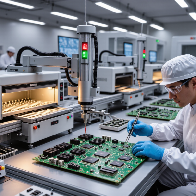
The work commonly includes solder-paste printing, component placement, reflow soldering, and inspection. For through-hole parts, technicians may use wave soldering or selective soldering. Automated optical inspection can reveal shifted components, solder bridges, or missing parts. X-ray inspection helps examine hidden joints beneath packages such as BGAs. As electronics manufacturing expert Michael Ford’s practical guidance can be summed up: “Reliable assembly begins with controlled processes and clear data.” The sentence is a useful reminder, though no process removes every risk.
Good assembly starts before the production line runs. Engineers review the board layout, component availability, thermal needs, and assembly tolerances. A test board may reveal a problem that looked invisible on a screen. That matters. Teams also document inspection criteria and process settings, so later batches can be compared with earlier ones. Still, a clean inspection is not proof of perfect field performance. That distinction deserves attention. Understanding Pcb Board Assembly helps buyers and engineers ask better questions about materials, process control, testing, and traceability. The result is not merely a populated board; it is a product built through choices that can be checked, measured, and improved.
What PCB Board Assembly Means
What Is PCB Board Assembly?
What PCB Board Assembly Means
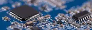
PCB board assembly is the process of turning a bare circuit board into a working electronic unit. The board provides conductive paths, while attached components perform tasks such as controlling power or processing signals. Assembly connects these parts to the board in a planned arrangement.
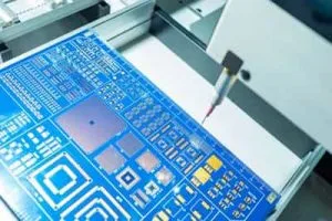
For surface-mount components, solder paste is placed on small copper pads, and automated equipment positions parts on top. The board then passes through a controlled heating process that melts the solder. Larger components may use through-hole assembly, where leads pass through drilled holes and are soldered in place. Tiny parts, tight spacing, and uneven heat can all affect the result. Small details matter.
Inspection may include checking component placement, solder joints, and electrical connections. A camera can spot a shifted part, but it cannot confirm every circuit works as intended. Functional testing adds another check by applying power or signals and measuring the board’s response. A clean-looking board can still contain a hidden fault.
Assembly quality depends on design, materials, equipment settings, and careful process control. There is no single setting that suits every board; a thick board and a dense, delicate one may need different handling. Even a well-managed process has limits, so testing and review remain important.
What Is PCB Board Assembly? – What PCB Board Assembly Means
| Dimension | What It Means | Typical Details |
|---|---|---|
| Definition | PCB assembly, often called PCBA, is a printed circuit board populated with electronic components and soldered to create a functioning electronic unit. | The assembly combines a fabricated board, components, solder joints, and any required inspection or testing. |
| Bare PCB vs. PCBA | A bare PCB has conductive patterns and board materials but no mounted electronic components. A PCBA has components installed and electrically connected. | A bare board is a substrate for assembly; a completed PCBA can perform a circuit’s intended function when correctly designed and integrated. |
| Common components | Assemblies may contain active and passive electronic parts. | Examples include integrated circuits, resistors, capacitors, connectors, diodes, and switches. |
| Surface-mount technology (SMT) | SMT components are placed onto conductive pads on the board surface and soldered in place. | A common process uses solder paste, component placement, and heating in a reflow oven to form solder joints. |
| Through-hole technology (THT) | Component leads pass through drilled holes in the board and are soldered to pads, usually on the opposite side. | THT may be assembled by hand or by a suitable soldering process; it is often used where a component’s mechanical attachment is important. |
| Mixed-technology assembly | A board may use both SMT and THT components. | The assembly sequence depends on component placement, board design, and the selected soldering methods. |
| Typical process steps | Assembly turns design and parts into a populated board through a controlled sequence of operations. | Typical steps include preparing the board and parts, applying solder paste when needed, placing components, soldering, inspection, and electrical or functional testing as specified. |
| Inspection and testing | Checks help assess component placement, solder-joint quality, and electrical behavior. | Methods can include visual inspection, automated optical inspection, X-ray inspection for suitable hidden joints, and in-circuit or functional testing. |
| Finished result | The result is a populated circuit-board assembly ready for the next manufacturing or integration step. | Depending on the product, it may be installed in an enclosure, connected to other assemblies, or used as a module within a larger system. |
Related Posts
-
7 Essential Tips for Sourcing the Best Quick Turn PCB Boards Globally
-
Global Procurement of Top-Tier PCB Prototype Boards: China's Manufacturing Excellence Unleashed
-
Innovative Approaches for Optimal Pcb Board Fabrication Success
-

Top Strategies for Optimizing Your Printing Circuit Boards Production Process
-
How to Select the Right Quick Turn PCB Boards for Your Project Needs
-
Maximizing After Sales Support and Minimizing Repair Costs with Best PCB Prototype Board Solutions