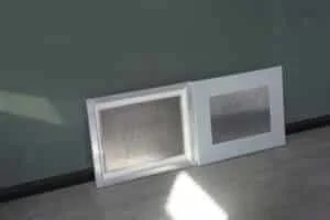
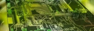


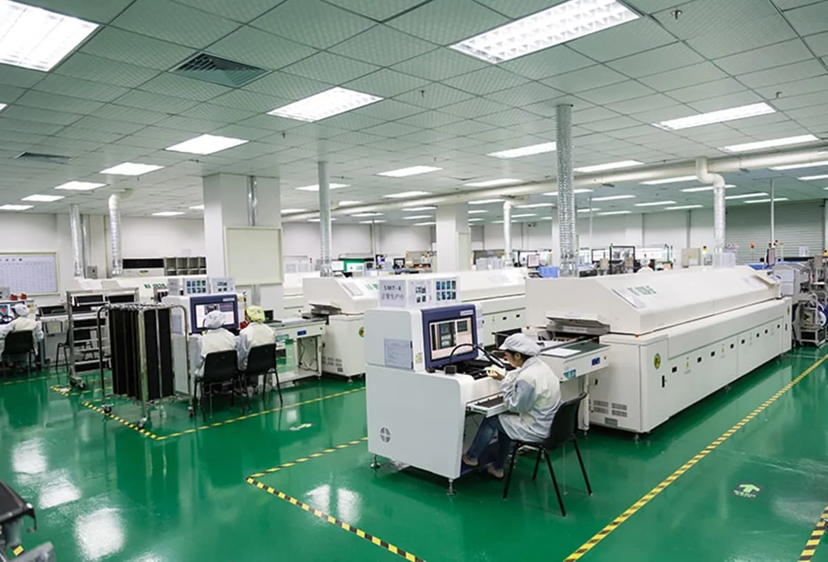
Does the SMT (Surface Mounted Technology) production line need to control the amount of dust in the environment? How does falling dust affect quality?
Why does the customer requirements to control the environmental pollution of the SMT production line?
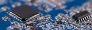
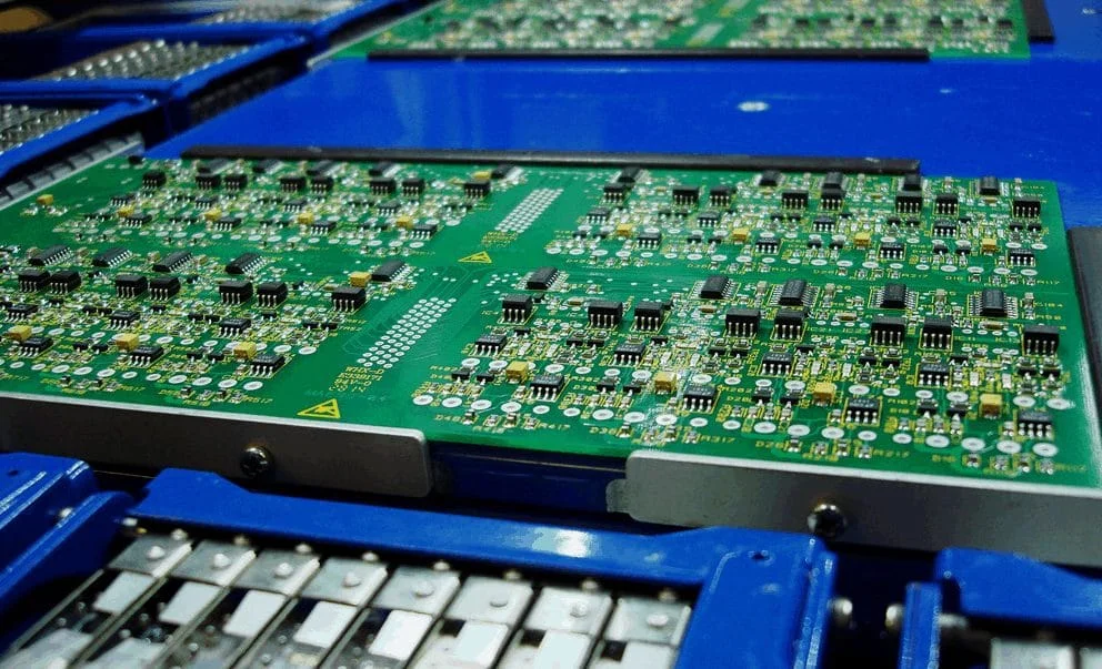
The most important thing for SMT production lines to control environmental dust is cotton wool, fibers, paper scraps, hair, dandruff, and other pollutants, not those tiny particles as small as 0.3um or 0.5um as everyone thinks. These contaminants do also cause quality problems in solder paste printing and soldering.
The possible effects of contaminants on the SMT process are as follows:
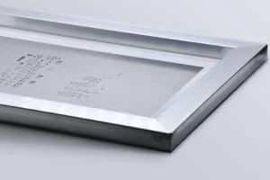
1) When the pollutants fall on the PCB Stencil, it will block the printing effect of the solder paste and cause a lack of tin;
2) When the pollutants fall on the PCB panel, it may raise the Stencil, increasing the amount of solder paste or burning and black spots during reflow, resulting in solder voids or poor tin eating, and even affecting the reliability of the product.
3) The glass fiber of the PCB falls between the pads, which may cause a short circuit of the solder or form a channel for electromigration in the future.
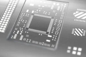
4) When contamination occurs in the solder joints of small chips such as resistors, capacitors, inductors, etc., the tombstone effect may occur because it will worsen the uneven tensile stress of molten tin.
5) When contaminants fall on top of the part body, it may affect the sealing of the pick-and-place machine nozzle and cause material throwing, which affects the activation of the pick-and-place machine. If too much dust is attached to precision instruments, it may affect the accuracy and life of the machine because these devices are driven by bearing screws. However, it seems that equipment manufacturers will do essential dust proofing.
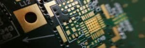
The above contaminants may not cause problems when the solder joints of the parts are still significant, but they can be problems in fine-pitch parts or BGA soldering and can also be a ticking time bomb.
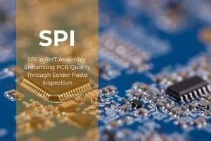
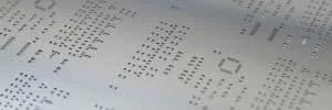
In addition, the size of the above pollutants is not large. It is generally not easy to check with the naked eye if you do not look carefully. Even if you import SPI (Solder Paste Inspection), you may not be able to check it out.
Therefore, the SMT production line must at least implement the following disciplines to control the above pollution sources:
1. It is strictly forbidden to open the carton packaging in or near the SMT production line. Because the dust from the carton is the most severe source in the current statistics, we think many small companies should do but fail to do, but it is also the easiest to do. The best way is to separate the SMT line from the carton unpacking.
2. Cotton batts or fibers may fall from the clothes worn by operators and engineers on the production line, which is one of the reasons why SMT production lines should wear anti-static clothing and dust-free caps.
3. Glass fibers that may fall from the circuit board. Glass fiber is one of the essential elements that make up the PCB, so when cutting the PCBA board, try to stay away from the SMT production line because the glass fiber and filler dust contained in the PCB will fall and fly when the PCBA board is cut.
4. To minimize the dust and pollutants brought by the external environment, it is recommended to have sticky dust pads and door blower dust removal devices.
In fact, the above requirements can be achieved as long as you usually make 5S (sorting, rectification, cleaning, cleaning, and literacy) and discipline management of the production line, as well as a small investment. Since SMT needs to control the cleanliness of the environment, we must give specific standards to measure the effectiveness, and the control of dust fall is a quantifiable and universal industrial standard at present.
However, most SMT production lines require that the amount of dust in the environment to be controlled does not need to reach a cleanroom level, but only to an environment similar to a “clean room.” Start with falling dust particles above 10um, and then gradually tighten the specifications according to demand and capacity. (The diameter of the hair is about 30-50um).
Finally, with the miniaturization of parts, if your SMT production line has plans or is already producing 0201 or even smaller 01005 or flip-chip components, it is recommended to raise the level of falling dust even further reduce the size of micro dust particle control.
Recommended Posts
The historical timeline and outlook of printed circuit boards
The origin of electronics can be traced back to 1897. Electromagnetic waves are the cornerstone of interconnection and communication between electronic components, and the invention of electronic tubes gave birth to PCBs.
Understanding Plated Through Holes (PTH) for Printed Circuit Boards
Plated through holes (PTHs) are vital in printed circuit boards for enabling reliable connectivity between layers. This article explores PTHs in depth—from their key benefits like durable interlayer connections and flexible component placement, to critical design considerations around hole size, spacing, depth. We also contrast PTHs to cheaper non-plated holes, and overview popular alternatives like blind and buried vias and their ideal use cases. For PCB designers and manufacturers, our insights help inform effective PTH integration tailored to your product requirements. Reach out to explore our professional PCB fabrication utilizing PTHs.
Evaluating and Selecting Quick-Turn PCB Assembly Manufacturers in China
This guide examines capabilities assessments and China region fit considerations for OEMs seeking quality quick-turn PCB assembly manufacturing between prototyping and early-stage production for electronics headed for Chinese end-markets.
What does PCB open Circuit Mean?
PCB open circuit is a problem that every PCB manufacturer encounters almost every day, plagued by production and quality management personnel. Insufficient shipments, replenishment, delivery delays, and customer complaints caused by PCB open circuits are difficult problems for the industry.
What Is Rogers Material PCB?
There is no doubting that fact that Rogers is one company that has managed to stand out amongst others in manufacturing laminate materials that are used in today’s circuit board. Printed circuit boards fabricated from Rogers materials offers strong moisture absorption and better thermal management.
What Are The Multilayer PCB Applications?
Due to the surprising benefits of multilayer PCBs, they are widely used in different industries. Firstly, it is the top priority of designers to implement their complex circuits, so wherever complex operation is required, these PCBs are used.